Optimizing Winding Interleaving in Planar Transformers: How Layer Ordering Drives High-Frequency Efficiency
 Two transformers. Same core. Same switching frequency. Same copper weight. One runs cool at full load; the other gets hot enough to trigger a thermal derating. The difference? One was designed with interleaving. The other wasn't.
In a multi-layer planar transformer operating at 500 kHz, AC resistance can exceed DC resistance by a factor of five to ten if the winding stack is not deliberately designed to manage proximity effect losses. A well-interleaved design at the same frequency can achieve an Rac/Rdc ratio close to 1.5. The delta in copper loss between these two extremes often determines whether a converter hits its efficiency target or misses it.
Why DC Resistance Is Only Half the Story
At DC and low frequencies, winding loss is simply I²Rdc. At high frequencies, two phenomena destroy that simplicity:
- Skin Effect: Current crowds toward the surface of the conductor within a depth δ = √(ρ/πfμ). In copper at 500 kHz, δ ≈ 93 µm. A 2 oz copper trace (70 µm thick) is slightly less than one skin depth, so skin effect alone is modest at this frequency.
- Proximity Effect: The dominant mechanism in multi-layer transformers. When conductors carrying opposing currents are adjacent (as primary and secondary inevitably are) the magnetic field of each induces eddy currents in the other, concentrating current into narrow bands. Loss scales with the square of the number of layers per winding portion. Double the layers → quadruple the proximity effect loss.
The MMF Diagram: Your Most Important Design Tool
The magnetomotive force (MMF) diagram plots the cumulative ampere-turn sum from bottom to top of the transformer stackup. The magnitude of the MMF at any layer interface is proportional to the proximity effect loss in adjacent conductors. High MMF peaks mean high losses.
Three configurations, three MMF profiles:
- Non-Interleaved (all P, then all S): MMF ramps up through all primary layers, peaks at the P/S interface, then drops through secondary. This is the highest-loss configuration.
- Fully Interleaved (P/2 -S - P/2): MMF ramps to NI/2 through the first half-primary, drops to zero through the secondary, ramps again through the second half-primary. Peak MMF is halved; since loss scales as MMF², proximity effect loss drops by a factor of four.
- Partially Interleaved: A controlled compromise: some layers crossed, not all. Reduces proximity effect while limiting the increase in inter-winding capacitance that full interleaving introduces.
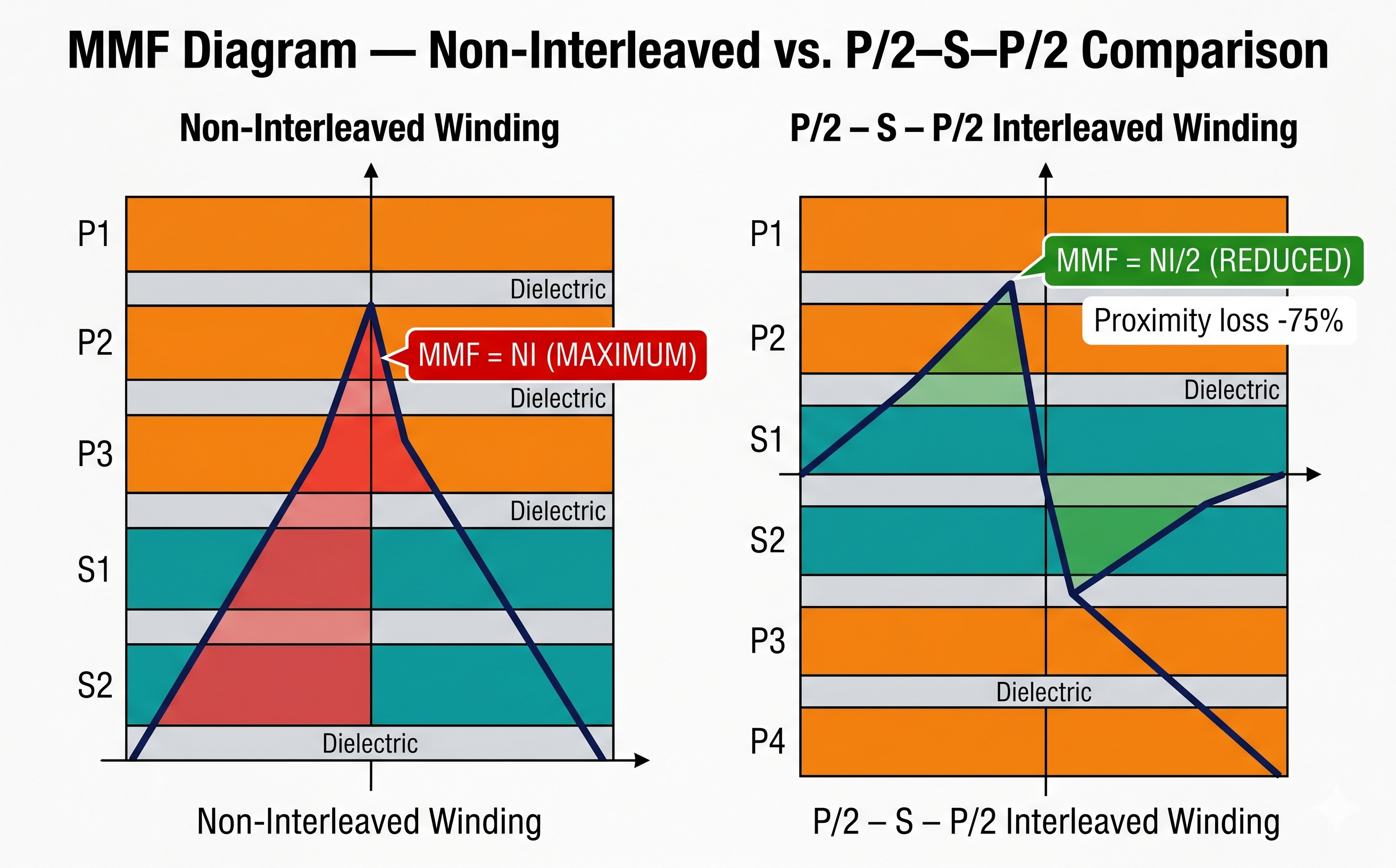
Non-Interleaved Winding (Left): This diagram shows all primary layers stacked above the secondary layers. The MMF builds to a maximal peak of NI at the boundary between the two, creating a large shaded red area that indicates high loss.
P/2-S-P/2 Interleaved Winding (Right): By splitting the primary layers and interleaving the secondary between them, the maximum MMF is effectively halved to NI/2. This leads to a significantly reduced shaded green area, resulting in a 75% reduction in proximity loss.
Winding Configurations in PCB Stackups
Full Interleaving: P/2 - S - P/2
The primary is split into two equal halves with the complete secondary sandwiched between them. The MMF diagram shows symmetric, low-amplitude peaks with zero net flux at the stackup center. For a transformer with 4 primary layers and 2 secondary layers, full interleaving typically reduces total winding loss by 60-80% relative to a non-interleaved design at the same frequency.
Secondary-Centered Interleaving: S/2 - P - S/2
Used when secondary current is the dominant loss source, common in step-down transformers with high secondary RMS current. The secondary is split and the primary is sandwiched. Equivalent loss reduction for the secondary winding.
Partial Interleaving
Only some layers are crossed. Offers a controlled compromise: reduced proximity effect with a smaller increase in inter-winding capacitance. The designer selects the optimal point on the loss-versus-capacitance trade-off curve for the application's EMI budget.
Quantifying the Benefit: Worked Example at 400 kHz
- Consider a 10:1 step-down planar transformer with the following parameters:
- Primary: 10 turns across 5 PCB layers (2 turns/layer), 1 oz copper (35 µm)
- Secondary: 1 turn, 1 PCB layer, 2 oz copper (70 µm)
- Operating currents: Primary 2A RMS, Secondary 18A RMS
- Switching frequency: 400 kHz
| Configuration | Dowell Factor (Primary) | Total Winding Loss | vs. Non-Interleaved |
|---|---|---|---|
| Non-Interleaved (5P | 1S) | ~3.8× | ≈ 4.2 W | — |
| Fully Interleaved (P/2–S–P/2) | ~1.4× | ≈ 1.6 W | −62% |
| Partially Interleaved (2P–S–3P) | ~2.1× | ≈ 2.6 W | −38% |
At 500W output power, that 2.6W saving from full interleaving represents a 0.5% improvement in converter efficiency - meaningful at system level across a production fleet.
Practical PCB Design Guidelines
- Copper weight selection: 1 oz copper (35 µm) often outperforms 2 oz above 300 kHz, thinner conductors suffer less proximity effect amplification despite higher Rdc. Calculate the crossover frequency for your geometry before defaulting to thicker copper.
- Via placement for current sharing: Vias connecting parallel layers must be placed symmetrically and uniformly. Asymmetric placement creates current crowding in specific layers, partially negating the benefit of parallel construction.
- Stackup symmetry: Mirror the stackup about the center plane. This minimizes net magnetic dipole, reduces leakage inductance variation, and ensures balanced heating across all PCB layers.
- Leakage inductance coordination: Interleaving reduces leakage inductance. In resonant converters (LLC, CLLC) where leakage is a tuned circuit element, the interleaving strategy must be coordinated with the required leakage value from the first design iteration — not retrofitted.
When Interleaving Isn't Enough
For converters above 1 MHz, additional techniques become necessary:
- Multiple thin parallel layers: Replace one thick layer with several thinner layers in parallel, Litz-wire behavior at the PCB level. Each thin layer carries less current and has a lower Rac multiplier.
- Distributed air gaps: Spread the core gap across multiple smaller gaps to reduce fringing flux concentration and localized eddy current losses adjacent to the gap.
- Core material selection: MnZn ferrites optimized for 500 kHz-3 MHz operation (3F4, N97, PC200) reduce core loss so that winding loss optimization remains the dominant efficiency lever.
Conclusion: The Stackup Is the Design
In a planar transformer, the PCB layer stack is not a packaging decision, it is the winding design. Every layer order, copper weight, and via placement has electrical consequences that determine whether the converter meets its efficiency targets or falls short.
Winding interleaving is the highest-leverage technique available. It costs no additional material, adds no assembly complexity, and can reduce winding loss by more than half. At Payton Planar, interleaving strategy is part of every custom transformer design. Contact us to discuss your design.