Creepage and Clearance in Multi-Layer PCBs: Why Safe Isolation Starts in the Stack-Up
 A gap of 0.3 millimeters. That's all that stands between a functioning power system and
a catastrophic high-voltage breakdown in a poorly designed multi-layer PCB. In the
world of planar transformer design, creepage and clearance aren't just numbers on a datasheet, they're the invisible architecture of electrical safety.
As power electronics continue their relentless march toward higher voltages and smaller footprints, the challenge of maintaining adequate isolation inside a multi-layer PCB has become one of the most consequential design decisions an engineer can make.
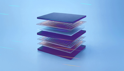
Planar transformers compress what was once a tall, wound-wire assembly into a low-profile, high-density structure. That compression brings incredible benefits and serious isolation challenges that demand both technical precision and regulatory fluency.
What Creepage and Clearance Actually Mean
These two terms are often used interchangeably, but they describe entirely different failure mechanisms.
Clearance is the shortest straight-line distance through air between two conductive parts at different potentials. Air itself is an insulator, until it isn't. At sufficient voltage levels, air ionizes and creates a conductive arc. The higher the voltage and the more contaminated the surrounding environment, the shorter the distance required to trigger this event.
Creepage is the shortest distance along the surface of an insulating material between two conductors. This one is trickier. Even a solid insulator like FR4 can allow surface current to creep, especially in the presence of moisture, dust, or ionic contamination. Over time, repeated surface discharges can form a carbonized tracking path, causing a permanent short circuit.
Both distances must be independently calculated and respected. Satisfying one does not satisfy the other.
Why Multi-Layer PCBs Complicate Everything
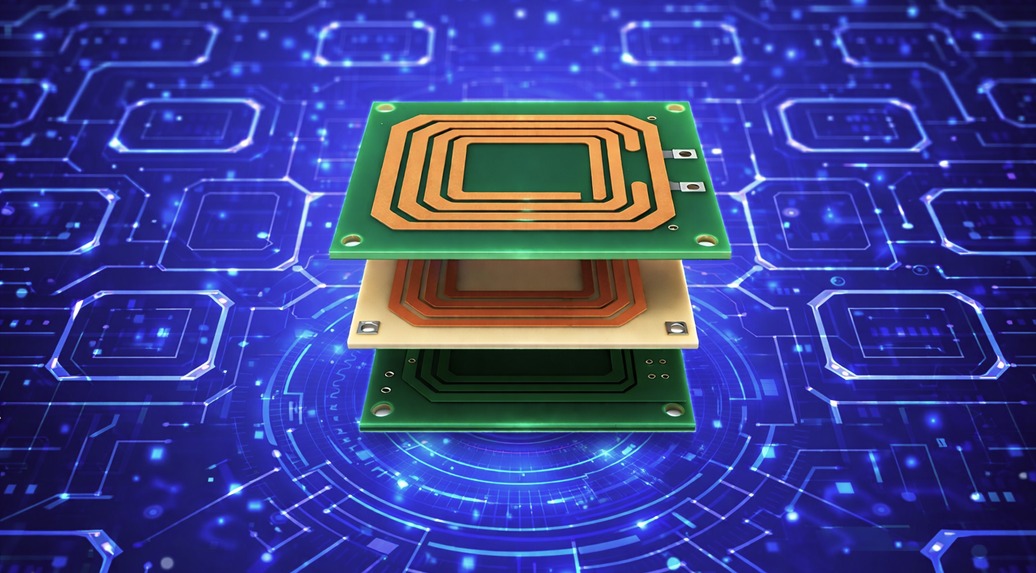
In a conventional wire-wound transformer, winding layers are physically separated with tape, bobbin flanges, and deliberate air gaps. Creepage and clearance management is relatively straightforward. In a multi-layer planar transformer PCB, the geometry shifts entirely.
Here's the core challenge: primary and secondary windings are etched onto adjacent copper layers, separated only by thin dielectric prepreg or core laminate, often as thin as 100-200µm. The insulation distances that safety standards demand must now be achieved within, across, and around a tightly packed board stack-up.
The key differences that complicate isolation in multi-layer PCBs:
- Reduced physical space. The entire transformer assembly may be only 5-10 mm tall. Every fraction of a millimeter counts.
- Multiple conductor layers. Primary windings, secondary windings, and auxiliary circuits may occupy four, six, or eight layers - each one a potential isolation boundary.
- Interlayer vs. surface distances. Safety standards treat creepage (surface) and internal insulation (through-laminate) distances differently, and both must comply simultaneously.
- Mixed voltage domains. A single board may carry both low-voltage control signals and high-voltage power conversion paths, requiring careful spatial segregation.
The Standards That Govern These Distances
Ignorance of the applicable standard is not a defense. Before a single trace is routed, engineers must identify which regulatory framework governs their product.
The most relevant standards for planar transformer PCB design are:
- IEC 60664-1: The foundational standard for insulation coordination in low-voltage systems. It defines clearance and creepage requirements based on working voltage, overvoltage category, pollution degree, and material group.
- IEC 62368-1: The current safety standard for audio/video, IT, and communication equipment, replacing the older IEC 60950-1. It introduces the Hazard-Based Safety Engineering (HBSE) approach and defines energy source classes that directly inform isolation requirements.
- IPC-2221A: The PCB design standard provides trace spacing guidelines, widely referenced alongside IEC standards for board-level compliance.
- UL 60950-1 / UL 62368-1: The North American equivalent certifications, essential for products sold in the US and Canadian markets.
A critical variable across all these standards is the Comparative Tracking Index (CTI) of the PCB surface material. CTI determines which "Material Group" your laminate falls into (I through IIIb), and this directly affects the minimum required creepage distance. FR4, the most common PCB substrate, typically falls into Material Group II or IIIa, which carries stricter creepage requirements than higher-performance laminates.
The Four Variables That Determine Your Required Distances
Getting creepage and clearance right is not a matter of guesswork or rule-of-thumb. The required distances are a calculated output of four input variables:
- Working Voltage - This is the maximum RMS or peak voltage that appears across the insulation boundary under normal operating conditions. It is not the supply rail voltage, it is the actual voltage stress seen at the specific isolation point in question.
- Overvoltage Category (OVC) - IEC 62368-1 defines four overvoltage categories (OVC I through OVC IV), reflecting the transient overvoltage a circuit is likely to experience. A main-connected switching power supply primary typically operates at OVC II or OVC III, which demands significantly larger clearances than a secondary-side low-voltage circuit.
- Pollution Degree (PD) - This variable accounts for the environment in which the PCB will operate. A sealed, clean indoor enclosure is Pollution Degree 1. An industrial environment with conductive contamination risk is Pollution Degree 3. Higher pollution degrees require longer creepage distances because contaminants facilitate surface tracking.
- Altitude - At altitudes above 2,000 meters, air density decreases, and so does its dielectric strength. IEC 60664-1 provides specific multiplication factors for clearance at altitude. At 5,000 meters, for example, a clearance distance calculated at sea level must be multiplied by a factor of approximately 1.48. This is particularly relevant for aerospace and avionics applications where Payton Group's planar magnetics for harsh environments are deployed.
Practical Design Strategies for High-Voltage Isolation in Planar PCBs
Understanding the theory is one thing. Building a board that passes safety certification (the first time) is another. Here are the strategies that experienced PCB designers apply to multi-layer planar transformer designs:
Use Adequate Layer Count and Layer Sequencing
Never place high-voltage primary layers directly adjacent to low-voltage secondary layers without a deliberate isolation layer in between. An interleaved winding scheme (P-S-P or S-P-S) can improve EMI and reduce proximity losses, but it must be executed with clear isolation boundaries assigned to specific layers. Each inter-winding insulation layer must independently meet the required throat laminate distance specified by the applicable standard.
Route Slot Cutouts to Extend Creepage Paths
On the PCB surface, creepage distance must be measured along the actual contour of the surface, including around any gaps or slots. Routing a slot or cutout between high and low-voltage copper regions on an outer or inner layer is one of the most effective ways to increase the creepage distance without increasing the board footprint. The current must now travel around the slot, increasing the effective path length.
Apply Conformal Coating or Potting
IEC 60664-3 and IEC 62368-1 recognize that a properly applied conformal coating can reduce the effective pollution degree of a PCB surface: from Pollution Degree 2 down to Pollution Degree 1. This can meaningfully reduce required creepage distances, enabling more compact designs without sacrificing compliance.
Verify Dielectric Strength Through Laminate
While creepage governs surface paths, the through-insulation distance governs inter-layer breakdown voltage. IEC 60950 historically required a minimum of 400 µm of PCB material thickness for mains insulation between primary and secondary windings; 200 µm where mains insulation is not required. Modern standards reference specific dielectric strength values in V/µm, and laminate selection must be verified against these values - not assumed.
Design for Thermal Expansion
PCBs expand under thermal cycling. In high-power planar transformers, temperature rises can be significant: particularly under high current, high-frequency operation. Thermal expansion can cause microcracks in laminate materials, subtly reducing through-insulation integrity over time. Payton's Planar technology, with its short heat path geometry and excellent thermal conduction characteristics, is engineered to minimize temperature differentials that stress PCB insulation.
Common Design Mistakes and How to Avoid Them
Even experienced teams make isolation errors. These are the most frequently encountered:
- Measuring creepage to the nearest adjacent conductor rather than the most critical path. Always identify every conductor at a different potential within reach of a high-voltage node.
- Failing to account for solder mask. Solder mask is not considered an insulating material for creepage/clearance purposes by most major standards. Do not rely on it to bridge a spacing shortfall.
- Ignoring the board edge. Board edges are exposed surfaces. A high-voltage trace routed close to a board edge may have an inadequate creepage path to a conductive chassis or mounting hardware.
- Using standard FR4 where high-performance laminate is needed. In ultra-compact, high-voltage designs, standard FR4 may not provide sufficient CTI. Selecting a higher-grade laminate early in the design process is far less costly than a compliance failure late in development.
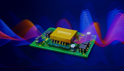
The Payton Advantage in High-Voltage Isolation
Creepage and clearance compliance is not an afterthought at Payton Group, it is a core design discipline embedded in every custom planar magnetics project. Payton's planar transformers feature a unique insulation solution engineered to deliver high-voltage isolation in an inherently compact, low-profile geometry. With a wide operating power range from 5W to 300kW and operating frequencies up to 2.5 MHz, Payton Group’s designs are fully compliant with international safety standards including UL certification.
Whether your application is industrial automation, electric vehicles, aerospace, or medical equipment, the isolation requirements are non-negotiable and the physical space available is shrinking. That is precisely the engineering challenge that Payton has solved across more than 25 years of planar magnetics development.
Conclusion: Small Distances, Large Consequences
Creepage and clearance in multi-layer PCBs demand the same rigor as any other electrical safety parameter, arguably more, because the consequences of failure are not gradual. They are sudden. Insulation breakdown in a high-voltage planar transformer can result in equipment destruction, fire risk, electric shock hazard, and failed certification.
The path to a safe, compliant design runs through four essentials: know your applicable standard, calculate all four input variables accurately, apply proven design strategies from the first layout revision, and select materials that meet dielectric requirements by a meaningful margin.
Your next step: If you're designing a high-voltage planar transformer assembly and need to validate your insulation strategy, contact Payton Group's engineering team for expert design consultation. With decades of experience in custom planar magnetics and a dedicated engineering support team, Payton can help you get compliance right, before the first prototype, not after.
--------------------------------------------------------------------------------