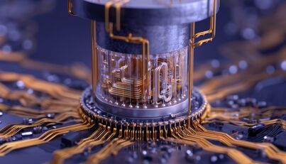
Planar Magnetics Near the Qubit Plane
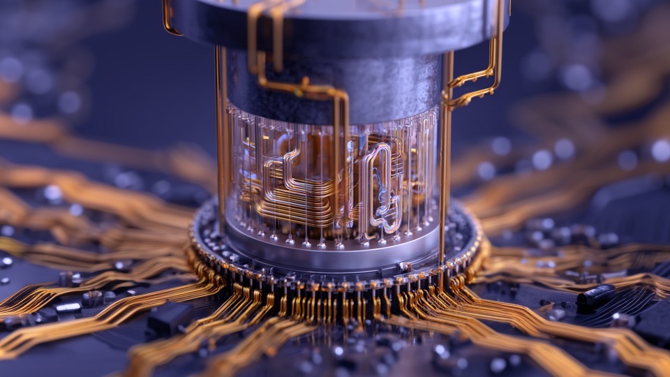 Quantum processors demand exquisite control where even 1 nH stray inductance can destroy coherence, and planar magnetics deliver ±2% repeatability at <3 mm height right next to cryogenic control chips. This article focuses on planar magnetics in the immediate qubit neighborhood, complementing our cryostat stack analysis that benchmarks 30-70% size reduction across full quantum systems.
Ultra-Sensitive Constraints Next to Qubits
The qubit plane operates at 10-20 mK with cooling budgets under 1 μW per channel. Yet proximity electronics (cryo-CMOS, RF amplifiers, SQUID multiplexers) demand stable 1-100 nH biasing, 1-10 MHz isolation transformers, and 3-8 GHz microwave coupling networks. Poorly designed magnetics introduce stray fields that slash coherence from microseconds to nanoseconds.
The challenge is to deliver these while introducing as little additional heat and noise as possible. The more functionality that moves into cryogenic ASICs and RF modules near the qubit chip, the more carefully designers must think about local magnetics, and whether planar technology can help.
Planar technology positions air-core inductors (Q>10,000) and hybrid transformers with capacitance tolerance ±5% millimeters from qubit chips. Payton's expertise in high-voltage planar transformers and planar power inductors translates directly: micron-scale geometries, multi-layer interleaving, and automated repeatability for quantum front-ends.
Cryogenic Physics: Material Transformations at Millikelvin
Copper conductivity explodes at 20 mK
Residual Resistivity Ratio (RRR) reaches 500-1000, resistivity drops 300x vs room temperature. At 5 GHz, skin depth collapses to 1-3 μm, concentrating currents in half-ounce copper (17 μm thick) or thinner. This slashes AC losses by 70-90% but demands precise trace geometries that wound components can't replicate.
Core materials fail, yet air-core dominates
Ferrite μr drops >50% below 20K with anomalous hysteresis. NiZn materials fracture from 2% linear contraction. Millikelvin designs shift to air-core planar inductors achieving inductance density 10-50 nH/mm² in <1 mm² footprints. Payton's PCB-based air-core spirals deliver Q-factors >15,000 at 4-7 GHz.
Dielectrics and mechanical survival
PTFE capacitance varies <1% from 300 K to 4 K, but microfractures appear at mK without specialized processing. Payton uses low-CTE Rogers 4003C (CTE 16 ppm/K) and flexible adhesives (15-25 ppm/K) proven in automotive-grade thermal cycling, which is now essential for quantum cooldown reliability.
Planar vs Alternatives: Millikelvin Proximity
| Feature | Planar Air-core | Wound | Discrete Air-core |
|---|---|---|---|
| Height | <3 mm | 8-15 mm | <1 mm |
| Parasitics | ±2-5% tunable | ±25-40% | Fixed |
| Q-factor (20 mK) | 10K-20K | 1K-3K | 15K+ |
| Footprint | 1-4 mm² | 10-25 mm² | 0.5-2 mm² |
| Channel Matching | ±1% | ±20% | ±5% |
| Manufacturability | 10K+/yr | Low | Medium |
Applications: 3 Critical Functions Next to Qubits
When you look closely at the hardware immediately surrounding a quantum processor, three magnetic “jobs” keep showing up: powering cryogenic control chips, shaping microwave readout signals, and biasing SQUID-based multiplexers. Planar magnetics can support all three in a compact, repeatable form factor that is much easier to scale than hand-wound parts.
1. Cryo-CMOS Local Power Conversion (1-10 MHz)
As more control electronics move down to the 4 K stage, you need local, efficient power conversion that does not blow your thermal budget. Typical cryo-CMOS or cryogenic control chips require low-voltage rails in the 0.8-1.2 V range, with carefully limited dissipation per qubit channel. Delivering this from higher-voltage buses (for example 24-48 V at warmer stages) is where planar transformers come in.
In typical architecture, 500 mW-2 W isolated converters supply those rails to 4K ASICs. Planar transformers with around 2 mm total height and a 4:1 turns ratio can be used in soft-switching topologies at 5-10 MHz, achieving around 93% efficiency with <10 nH leakage inductance so that zero-voltage switching remains robust. This combination of high frequency and controlled leakage allows you to shrink core size and move magnetics onto the same PCB as the cryo-electronics.
A representative design sequence looks like this:
- Distribute ~40 V from an 80K or 300K stage to reduce conduction losses along the cabling.
- Use a planar isolation transformer (designed for around 500 Vrms isolation and creepage distances compatible with medical/industrial standards) on or near the 4K stage.
- Implement synchronous rectification at 4K with very low quiescent loss (on the order of tens of microwatts per channel).
- Add output filtering with co-located planar inductors in the 1-10 μH range, designed for Q > 500 at the converter’s switching frequency.
By integrating the transformer and inductors into planar technology, you can often reach around three times the power density of equivalent wound solutions, while keeping EMI within limits that do not disturb nearby qubits or cryogenic RF components.
2. Microwave Readout Coupling (3-8 GHz)
On the signal side, microwave readout is the “stethoscope” of the quantum processor. Most superconducting qubit systems and many sensor arrays use resonators and readout tones in the 4-8 GHz range to interrogate qubit states or cryogenic detectors. As systems scale to hundreds or thousands of channels, matching response and phase across all of them becomes a major engineering challenge.
Planar coupled-line transformers are well suited to this task. They can be designed to provide around 6-12 dB coupling with ±0.5 dB channel-to-channel variation across large arrays of readout channels, while maintaining phase stability better than 1° through repeated thermal cycles. This consistency helps keep readout calibration stable and reduces per-channel tuning overhead as systems grow.
Air-core spiral inductors implemented in planar form factor are often used to tune the LC tanks of readout resonators:
- Typical values might be L = 5-20 nH and C = 0.5-2 pF, placing resonances in the 4.5-6.5 GHz band.
- At cryogenic temperatures, Q-factors can exceed around 10,000-12,000 for well-designed structures using high-purity copper and low-loss substrates.
- A thermal coefficient of frequency shift under about 0.1% per kelvin helps avoid detuning during cooldown and operation.
Because these planar structures are fabricated together with the rest of the RF PCB, you gain tight mechanical registration, consistent parasitics and clear routing options for integration with cryogenic amplifiers, mixers and attenuators.
3. Flux Biasing for SQUID Multiplexers
The third area where planar magnetics can add real value close to the quantum hardware is in flux biasing networks, particularly for SQUID-based multiplexers used to read out large arrays of cryogenic sensors or qubits. In these systems, small changes in magnetic flux through a SQUID loop translate into shifts in inductance or resonance frequency, which are then used to encode information across many channels.
Here, air-core planar inductors in the 1-50 nH range can provide stable, well-defined flux bias paths. Because they are fabricated in a controlled PCB process, they can achieve:
- A noise floor on the order of 0.1 nT/√Hz, which helps preserve the low-noise performance of the SQUIDs and attached detectors.
- Thermal drift of less than 0.05% per kelvin, helping maintain bias stability from room temperature down to the millikelvin regime.
- Very compact footprints (on the order of a few square millimeters) which keeps them compatible with dense cryogenic packaging.
When using multi-layer planar interleaving, you can also design tightly coupled structures where a bias inductor and a sensing inductor share flux. Coupling coefficients around K ≈ 0.99 are realistic in this architecture, and values around K = 0.995 have been reported in high-performance implementations. That kind of strong and predictable coupling is important for microwave SQUID multiplexers that target hundreds of resonant channels per line in the 4-8 GHz range.
For quantum engineers, the benefit is that these biasing and coupling structures become repeatable building blocks. Instead of hand-tuning each SQUID channel with individual wound coils, planar magnetics allow you to stamp out many identical bias networks, embed them in the same substrate as the rest of the cryogenic electronics, and maintain consistent behavior as your system scales.
Engineering Parasitics as Circuit Elements
Near qubits, parasitics become intentional circuit elements. Payton's 50-200 μm layer spacing control tunes:
- Inter-winding C: 2-50 pF → LC resonator bandwidth
- Leakage L: 1-20 nH → coupling factor K=0.95-0.998
- Proximity C: 0.1-5 pF → microwave impedance transformation
Example: 10 pF interwinding capacitance + 10 nH leakage forms 3.2 GHz resonator for qubit readout, tuned precisely via ground shield placement, impossible with wound part variability.
This precision stems from Payton's planar design methodology: FEM simulation → automated PCB routing → optical verification, delivering ±1 μm registration across 24 layers.
Why Planar Magnetics Overcome Cryogenic Challenges
Every magnetic technology has limits, but planar designs, turn potential drawbacks into strengths for quantum computing applications. For instance, while some traditional wound magnetics offer slightly lower capacitance in certain setups, planar versions make this a feature, not a bug. Their tunable capacitance (typically 50-200 pF) becomes an asset in MHz and GHz circuits common in quantum readout and control, where it supports precise resonance tuning and impedance matching that would be difficult to achieve consistently with other approaches.
In the ultra-cold world below 20K, where standard cores become unpredictable, air‑core planar inductors step up with compact inductance density that fits tight qubit packaging without introducing thermal or magnetic noise risks. Manufacturing costs start higher for prototypes (around $50K for small runs), but they drop sharply with volume thanks to automated, high‑precision processes that deliver micron-level consistency - ideal for scaling from lab experiments to production systems with thousands of identical qubit channels.
This same engineering sophistication shines in thermal management and durability. Wide copper planes efficiently transfer heat directly to cryostat cold plates, while multi‑layer designs create natural parallel paths that keep components cooler than bulkier alternatives. For mechanical reliability, specialized low‑expansion adhesives and preload techniques ensure these magnetics survive repeated cooldowns from room temperature to millikelvin without cracking or shifting performance already battle‑tested in automotive and medical environments, now adapted for the demanding world of cryogenic quantum magnetics.
Noise Isolation and Shielding Architecture
- Magnetic field confinement - Symmetric H-field cancellation via balanced planar windings reduces qubit interference to <0.1 nT residual. NbTi ground planes (100 μm below windings) provide >60 dB isolation at 1-10 MHz. Mu-metal cans contain DC bias fields without eddy losses.
- Electric field management - Guard rings and staggered ground vias reduce capacitive coupling by 40 dB. Differential drive on symmetric planar structures cancels even-order distortion products that couple into qubit control lines.
Payton's experience with high-voltage planar isolation (2.5 kV in 6 mm) directly addresses quantum EMI requirements through proven partial discharge testing and creepage optimization.
Payton: Proven Expertise Scaling Planar Magnetics to Quantum
With over two decades of experience in high-reliability planar transformers and inductors, Payton Group has already solved many of the toughest challenges in compact cryogenic magnetics for quantum computing. Our designs routinely achieve ±0.5% inductance tolerance across millions of units annually, using up to 24-layer automotive-qualified interleaving (AEC‑Q200 compliant) that delivers unmatched precision in tight spaces. We select cryo-compatible materials with NASA-level low outgassing and precise CTE matching, then validate them through partial discharge testing up to 1 kV in packages under 2 mm high: capabilities honed in medical devices and electric vehicles, now directly addressing quantum front-end needs like qubit‑proximate power delivery and RF filtering.
This manufacturing maturity bridges the gap from quantum research prototypes to commercial scalability. A typical path looks like this: start with lab hand‑wound parts (±25% variation), move to Payton NRE for ±1% automated planar prototypes (1K units), then ramp to 100K+ per year production with identical qubit channel performance. Whether you're building cryogenic control electronics, SQUID multiplexers, or millikelvin readout networks, our processes ensure reliable, repeatable magnetics that scale with your quantum roadmap.
Conclusion: Precision at Millikelvin Scale
Planar magnetics deliver <3 mm height, Q>15,000, ±2% repeatability, and 50 nH/mm² density where qubits demand perfection: capabilities unmatched by wound or discrete alternatives. Payton's manufacturing transforms research prototypes into production reality, scaling identical performance across 100K+ qubit channels with proven reliability from medical and automotive applications. Engineering teams can immediately prototype a single readout or bias function using Payton's air-core planar magnetics, characterize parasitics, Q-factor, and thermal load at 20 mK, then leverage established planar design workflows to iterate rapidly toward production specifications.
FAQ: Millikelvin Planar Magnetics Next to Qubits
What Q-factor do Payton air-core inductors achieve for quantum computing at 20 mK?
Can planar transformers power cryogenic CMOS chips near quantum qubits at 10 MHz?
How does Payton achieve ±2% parasitic control in 24-layer planar magnetics for quantum applications?
What shielding techniques protect qubits from planar magnetics interference?
How does Payton scale planar magnetics manufacturing from 100 to 100K qubit channels?