Transitioning from Conventional to Planar Transformers
 It performs. It passes testing. It ships in the product. And yet, every engineer who has wrestled a bulky wire-wound transformer into a shrinking PCB footprint knows the feeling: there must be a better way. There is! and it's been quietly transforming power electronics design for over two decades.
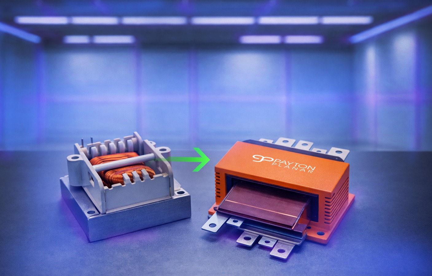
Converting an existing wire-wound transformer design to a planar transformer is one of the highest-leverage design decisions available to a power electronics engineer. Smaller footprint, better thermal management, higher efficiency, superior repeatability: the benefits are well-documented and substantial. But the transition requires a disciplined, step-by-step process. This guide walks you through exactly that.
Why Engineers Make the Switch: The Case for Going Planar
Before diving into the how, it's worth being clear about the why, because understanding the motivation shapes every design decision that follows.
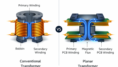
Planar transformers replace hand-wound wire coils on a bobbin with flat, etched copper windings on a multi-layer PCB. The physics of magnetics don't change: the same ferrite cores, the same fundamental relationships between turns, flux, and inductance all apply. What changes is the construction geometry, and that change cascades into a wide range of measurable performance improvements.
Here's what engineers consistently gain in the conversion:
- Power density up to 3× higher than conventional wire-wound designs, enabling a dramatically smaller component at the same power level.
- Efficiency is typically 98-99%, compared to 92-96% for many wire-wound designs at equivalent power levels.
- Dramatically reduced profile - a critical advantage in modern power converter layouts where height is the most constrained dimension.
- Superior thermal conduction through a short, direct heat path from PCB winding to heatsink or chassis.
- Exceptional manufacturing repeatability - pre-tooled PCB windings eliminate the variance inherent in hand-wound production.
- Lower EMI emissions through tightly controlled winding geometry and optimized shielding.
If your current design is constrained by any of these parameters: size, heat, efficiency, or production consistency - the conversion is worth doing. Let's get into the process.
Step 1: Audit Your Existing Design
Don't start with a blank sheet. Start with a thorough audit of the wire-wound design you're replacing. The goal is to extract every electrical parameter that the planar design must replicate or improve upon.
Document the following before touching a schematic:
- Input and output voltages (min, nom, max)
- Output power and current per winding
- Switching frequency and topology (flyback, LLC, phase-shifted full bridge, forward, etc.)
- Turns ratio for each winding
- Primary inductance (magnetizing inductance)
- Leakage inductance (measured, not calculated, they often differ in wire-wound designs)
- DC resistance of primary and secondary windings
- Isolation voltage requirements between primary, secondary, and any auxiliary windings
- Operating temperature range and thermal constraints
- Applicable safety standards (UL, IEC 62368-1, EN 50155, etc.)
This audit serves a dual purpose. It gives you the target specification for the planar design. It also often reveals that the original wire-wound transformer was over-designed in some parameters and under-designed in others, insights that allow you to optimize the planar version rather than simply replicate the wire-wound one.
Step 2: Evaluate Whether Your Topology and Frequency Are Planar-Ready
Planar transformers are optimized for high-frequency switch-mode power supplies (SMPS). This matters because your switching frequency directly determines how easily the conversion can be made and whether it requires a topology adjustment.
Frequency Is Your Friend
The higher the switching frequency, the fewer turns are required to achieve the necessary volt-seconds on the core. Fewer turns mean fewer PCB layers, a thinner stack-up, and a smaller overall footprint. If your existing design runs at 20-100 kHz, it is already well within the planar transformer's natural operating range of 20 kHz to 2.5 MHz. If it runs below 20 kHz, a frequency increase may be warranted, and this is the moment to evaluate that possibility.
Topology Compatibility
Most common SMPS topologies are fully compatible with planar magnetics: flyback, forward, LLC resonant, phase-shifted full bridge, and active clamp forward are all well-established in planar form. LLC resonant topologies in particular pair exceptionally well with planar transformers because their soft-switching behavior minimizes the impact of the slightly higher inter-winding capacitance that can accompany planar construction at high layer counts.
If your existing design uses a topology that's a poor match for high-frequency operation, this is the right time to reconsider, not after you've committed to a core geometry.
Step 3: Select the Right Planar Core
Core selection is where the planar design diverges most sharply from the wire-wound process. Planar cores (typically E-E or E-I ferrite pairs with a low-profile geometry) come in standardized sizes with defined window areas and effective core cross-sections. Your job is to match the core to your power and frequency requirements.
Use the Area-Product (AP) Method
The area-product method (the product of the core's window area and its cross-sectional area) provides a reliable starting point for core sizing in planar designs, just as it does for wire-wound ones. A core's AP value must be large enough to accommodate the required copper cross-section for all windings at the chosen current density.
Key Core Selection Criteria
- Effective core area (Ae): Determines the required number of turns via Faraday's Law at the operating frequency and peak flux density.
- Window area (Aw): Determines how many PCB winding layers can physically fit within the core aperture.
- Core material grade: Higher-frequency designs require low-loss ferrite grades (such as 3F3, 3F4, or equivalent) to control core losses at the target switching frequency.
- Saturation flux density (Bsat): Your peak operating flux density should be comfortably below Bsat, typically targeting 50-70% of Bsat to allow thermal headroom.
A practical note: it is common to find that the planar core equivalent to your wire-wound core is one size smaller. Higher power density is the norm in planar designs, not the exception.
Step 4: Calculate Turns and Layer Stack-Up
With the core selected and the electrical specification in hand, you can calculate the number of turns for each winding. The primary turns are determined by Faraday's Law:
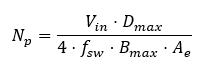
Where Vin is the input voltage, Dmax is the maximum duty cycle, fsw is the switching frequency, Bmax is the target peak flux density, and Ae is the effective core area.
Secondary turns follow from the turns ratio established in your original design. Round to the nearest integer, fractional turns are not achievable in planar designs and recalculate the turns ratio to confirm the output voltage is within specification after rounding.
Planning the Layer Stack-Up
This is one of the most consequential decisions in the entire conversion process. How turns are distributed across PCB layers affects leakage inductance, inter-winding capacitance, thermal distribution, and isolation compliance. Established best practices include:
- Interleave primary and secondary windings (P-S-P or S-P-S configurations) to reduce AC winding losses and leakage inductance.
- Assign dedicated isolation layers between primary and secondary winding groups: minimum 0.4 mm of dielectric for reinforced isolation.
- Distribute high-current windings across multiple parallel layers to manage current density: planar transformers support up to 200A per layer.
- Keep the stack-up symmetrical around the mid-plane where it is possible to minimize thermal gradients and mechanical stress.
Step 5: Design the PCB Winding Layout
With turns count and layer stack confirmed, the PCB winding layout brings the design to life. Each turn is a copper trace routed as a spiral within the core window area. Trace width, spacing, and copper weight are not arbitrary. They are calculated from current density, temperature rise limits, and the creepage and clearance requirements of the applicable safety standard.
Winding Layout Essentials
- Trace width: Calculate from the maximum RMS current per layer and the allowable current density, typically 4–6 A/mm² for a conservatively rated planar design.
- Copper weight: Standard PCB copper (1 oz/ft², 35 µm) is often insufficient for high-current layers; 2 oz (70 µm) or 3 oz (105 µm) copper is commonly specified.
- Via interconnects: Turns are connected between layers via vias. Use multiple vias in parallel at each inter-layer connection to minimize via resistance and improve current distribution
- Creepage and clearance: Maintain the distances required by your applicable standard between primary and secondary copper on the PCB surface and between layers, do not rely on solder mask as insulation.
- Ground planes and shielding: A shielding layer between primary and secondary windings, connected to the appropriate reference potential, can significantly reduce common-mode EMI, particularly important in isolated converter designs.
Validate Thermally Before You Build
Thermal validation is not optional. It is the step most commonly skipped and most frequently regretted. Before committing to a PCB fabrication, model the thermal performance of your winding design.
Copper losses in each winding layer are proportional to the layer's DC resistance multiplied by the square of the RMS current, plus AC winding losses due to skin effect and proximity effect at the switching frequency. At high frequencies and high copper weights, AC winding losses can significantly exceed DC losses and must be calculated using Dowell's method or an equivalent analytical approach.
Payton’s Planar technology is specifically engineered with a short heat path from the winding to the heatsink or chassis mounting surface. If your planar design is properly configured for conduction cooling, the thermal advantage over the wire-wound predecessor is substantial and predictable.
Prototype, Measure, and Iterate
Simulation and calculation get you close. Measurement gets you there. Build a prototype PCB, assemble it with the selected core, and measure the following parameters against your original specification:
- Magnetizing inductance - should match your calculated value within ±10%.
- Leakage inductance - typically 0.2% of primary inductance for well-designed planar transformers; significantly lower than most wire-wound designs.
- DC resistance - measure each winding individually; compare against calculated values.
- Turns ratio - verify at low signal levels before applying power.
- Isolation voltage - hi-pot test to the required level per applicable safety standard.
- Thermal performance - measure winding temperatures at full load; compare against thermal model predictions.
- EMI performance - measure conducted emissions at the converter output; compare against wire-wound baseline.
Iterate as needed. In most first-pass planar conversions, leakage inductance comes in lower than expected (a pleasant surprise), and thermal performance exceeds the wire-wound predecessor by a comfortable margin. If your converter topology was optimized around a specific leakage inductance value, as LLC resonant designs often are, you may need to adjust the resonant tank components to account for the change.
Conclusion: A Transition Worth Making…With the Right Partner
Converting from wire-wound to planar is not a redesign from scratch. It is a structured, methodical process that builds directly on the electrical specification you already have. The seven steps covered here: audit, topology review, core selection, turns calculation, PCB winding design, thermal validation, and prototype testing - give any power electronics engineer a clear path from an aging wire-wound design to a high-performance planar solution.
The performance gains are real: smaller, lighter, more efficient, more consistent, and better suited to the thermal and electromagnetic demands of modern power electronics applications.
FAQs: Converting Wire-Wound to Planar Transformers