How GaN Changes the Rules for Planar Magnetics
Gallium nitride (GaN) semiconductors switch up to 10x faster than silicon MOSFETs with near-zero reverse recovery charge and switching losses under 50% of equivalent silicon devices. This enables practical operation above 500 kHz (even into the low MHz) in isolated DC/DC converters where silicon previously hit diminishing returns.
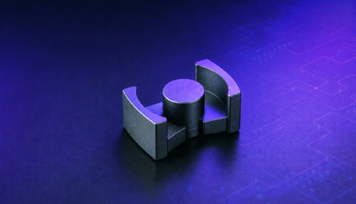
The payoff for planar transformer designers is direct: magnetics size scales inversely with frequency squared. A converter pushed from 100 kHz to 1 MHz can use 50-70% fewer turns and 30-50% smaller cores, shrinking footprint while maintaining isolation and efficiency. Payton's custom planar transformers are built for exactly this regime, combining PCB windings with optimized cores for GaN‑driven power supplies in medical, automotive, and industrial applications.
Planar vs Wire-Wound at GaN Frequencies
| Frequency | Planar Advantage | Key Challenge |
|---|---|---|
| <200 kHz | Lower profile | Limited size win |
| 200-500 kHz | Footprint -30% | Emerging copper loss |
| >500 kHz | Footprint -60% | Copper loss dominates |
From Silicon Limits to GaN Opportunities
 For years, silicon dictated how small and how fast isolated converters could realistically be. Switching losses and reverse-recovery behavior made it difficult to raise frequency much beyond about 100-200 kHz without taking an immediate hit in efficiency, thermal performance, and EMI. The result was a compromise: magnetics (especially in the 200 W to multi-kW range) often ended up larger and taller than designers wanted, particularly in automotive, data‑center and industrial supplies.
GaN fundamentally changes that equation. Thanks to much better switching figures of merit: lower gate charge, much lower output capacitance, and essentially zero reverse‑recovery - commercial GaN devices now support 500 kHz to 2 MHz operation in practical DC/DC topologies while still achieving around 95-97% efficiency. This isn’t just a lab claim; automotive-oriented 48 V-12 V GaN reference designs demonstrate higher efficiency at 250-800 kHz than silicon designs running at 100 kHz, with cooler operation and reduced magnetics size.
That frequency headroom transforms planar magnetics from “nice to have” into a very strong option wherever profile and power density matter. When a converter moves from 100 kHz toward 600-800 kHz, the allowable volt-seconds per turn drop by a factor of 5-8, so designers can use fewer turns, smaller cores, and tighter PCB windows. In practice, this often means a planar transformer can be 30-60% lower in height and significantly smaller in footprint than a comparable wire‑wound part, while still meeting isolation and efficiency targets.
Payton sees this trend directly in applications like automotive DC/DC conversion. For example, in a 48 V-12 V GaN-based converter operating in the 500-800 kHz range, a custom planar transformer can be designed with a single-digit millimeter profile: on the order of 6-8 mm total height versus 15-20 mm for many traditional wound solutions - freeing PCB area for parallel GaN switches, EMI filtering, or control circuitry. At the same time, the design still leverages the company’s experience in kW-class planar transformers at ~200 kHz for demanding industrial and AI power platforms.
In other words, GaN doesn’t make planar magnetics automatically “better” at high frequency, but it finally makes the tradeoff space wide enough that the size, profile and repeatability advantages of planar often outweigh the extra AC copper loss and capacitance, especially when you apply the kind of careful winding, layout and thermal design that Payton’s engineering teams use across their planar transformer families.
Why Higher Frequency Shrinks Planar Transformer Footprints
Pushing the switching frequency higher in a power converter fundamentally changes what your magnetics need to do. The required energy storage drops roughly as 1/f² (where f is frequency), and the peak flux density excursions scale inversely with f. For a fixed power level and ripple spec, this means you can get away with a much smaller core cross‑section (typically 30-50% reduction) along with 3-5x fewer turns and a proportionally smaller window area to fill with copper. The result is a transformer that takes up dramatically less PCB real estate and vertical height, which is especially valuable in dense automotive, medical, or server power applications where every millimeter counts.
Published GaN converter designs confirm this in practice, showing transformer volume reductions of 40-70% compared to silicon baselines running at lower frequencies. Payton’s planar magnetics already push power densities above 20 kW/L in optimized medical and industrial platforms under controlled thermal and airflow conditions. GaN takes these capabilities into even tighter envelopes, like compact EV onboard chargers or AI server bricks where profile constraints are non‑negotiable. With the right design, you’re not just shrinking the transformer, you’re unlocking system-level savings in enclosure size, cooling complexity, and bill of materials.
Of course, higher frequency isn’t a free lunch, particularly for planar magnetics. Above 500 kHz, AC copper losses from skin effect (current crowding to the surface) and proximity effect (field interactions between adjacent conductors) often become the dominant loss mechanism, sometimes exceeding core hysteresis and eddy current losses. Effective skin depth drops below 0.2 mm at these frequencies, forcing current into the outer layers of your copper conductors and raising resistance dramatically if you don’t adapt. Payton counters this through proven strategies like parallel winding layers (typically 2-4 per side), optimized copper thickness (70-200 μm foil or 4-6 oz PCB copper), and carefully interleaved primary/secondary arrangements to minimize proximity penalties. These techniques reliably keep total copper loss under 20% of output power even at 1 MHz, as demonstrated in their high‑power density planar transformers. The key is simulation‑driven optimization upfront, ensuring your GaN-planar combo stays cool and efficient where pure silicon could never reach.
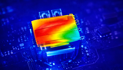
Thermal and Layout Benefits in High-Frequency Planar Designs
Shrinking the footprint is only half the story. As switching frequency and power density rise with GaN, thermal and layout challenges become more pronounced. Planar transformers help because their flat PCB‑based structure spreads heat laterally across large surface areas and provides predictable coupling to heatsinks or cold plates, unlike wound transformers where heat bottlenecks in wire bundles and tall bobbins.
However, GaN's fast dV/dt edges (50 V/ns) drive common-mode currents through planar's higher inter-winding capacitance (typically 2-5x wire-wound). Payton adds Faraday shield layers (tied to primary ground) that block >40 dB CM noise, plus dense via arrays and embedded copper planes for 0.5-1 W/K vertical thermal paths to prevent core hotspots. Engineers transitioning designs will find Payton's planar transformer design guide invaluable - it walks through core selection, PCB winding strategies, and thermal considerations specifically when moving from conventional to planar technology in high‑frequency applications.
Example: Payton's 8 kW, 200 kHz industrial planar transformer uses 12-layer shielded interleaving to achieve <50°C rise under GaN drive with CM emissions 30 dB below CISPR limits, proof that flat geometry plus smart layout delivers where tall magnetics struggle.
Design Considerations: Matching GaN Devices To Planar Magnetics
To unlock GaN’s full impact on planar footprints, magnetics design must be intentionally aligned with the semiconductor’s strengths.
Key considerations include:
- Target frequency selection: GaN often allows operation above 500 kHz or into the MHz region, but the “sweet spot” depends on topology, efficiency targets and EMI limits. The transformer must be optimized around this frequency, not simply scaled from a lower‑frequency design.
- Core material and geometry: At higher frequencies, ferrite losses rise quickly. Selecting suitable core materials and shapes for planar transformers is essential to balance losses against size reduction.
- Winding layout and parasitics: Planar structures offer fine control over leakage inductance, interwinding capacitance and coupling. This enables designers to intentionally shape parasitics to support resonant topologies or to minimize overshoot and ringing.
- Integration of inductors: Some GaN‑based converters use planar transformers with integrated resonant inductance, reducing part count and footprint compared to separate magnetics.
- Isolation and creepage: As frequencies rise, insulation design and creepage distances remain non‑negotiable, especially in medical or automotive systems. Planar constructions simplify adherence to standards while maintaining compact dimensions.
For projects moving from wire‑wound designs to GaN‑enabled planar architectures, collaborating with a specialist in custom planar magnetics, such as Payton Group, helps align transformer and inductor design with both the semiconductor roadmap and the regulatory environment.
Frequency-specific challenges
| Frequency | Core Loss | Copper Loss | Key Mitigation |
|---|---|---|---|
| 100-300 kHz | Dominant | Low | Standard ferrite |
| 300-800 kHz | Balanced | Rising | Interleaving |
| >800 kHz | Low | Dominant | Thin foil + shielding |
Application Domains Where GaN and Planar Footprints Matter Most
The impact of GaN on planar transformer footprints is not confined to small chargers. It is increasingly visible in:
- Medical power supplies: Where low profile, isolation and reliability are critical, planar transformers already offer strong benefits; GaN adds the ability to further shrink designs and reduce thermal stress.
- Automotive and e‑mobility: High‑voltage DC/DC converters and on‑board chargers are under constant pressure to increase power density. GaN and planar magnetics together support compact, efficient conversion stages suitable for electrified platforms.
- Industrial and data‑center power: As architectures migrate to higher bus voltages and more distributed conversion, high‑frequency planar transformers can help achieve the required power densities and serviceability.
- Compact adapters and fast chargers: Consumer power supplies are already leveraging GaN plus high‑frequency planar magnetics to deliver high wattage in surprisingly small enclosures.
In all these domains, the combination of GaN semiconductors with custom planar transformers and inductors creates a path toward smaller PCBs, lower profiles and higher power density without compromising safety or regulatory requirements.
Conclusion: One Next Step for Your Next Design
As GaN devices continue to mature, the pressure will only increase to revisit magnetics and reclaim the footprint savings that high‑frequency operation makes possible. Planar transformers and inductors are uniquely positioned to turn those semiconductor advantages into practical, manufacturable hardware that fits real‑world constraints.
If you are planning a new GaN‑based isolated converter or looking to migrate an existing silicon design to a smaller, higher‑frequency architecture, a practical next step is to review your existing transformer specifications using a dedicated planar design guide and engage a magnetics partner early to explore how far your footprint can realistically be reduced.