EMI/EMC Mitigation in Planar Magnetics: Built-In Advantages and Design Best Practices
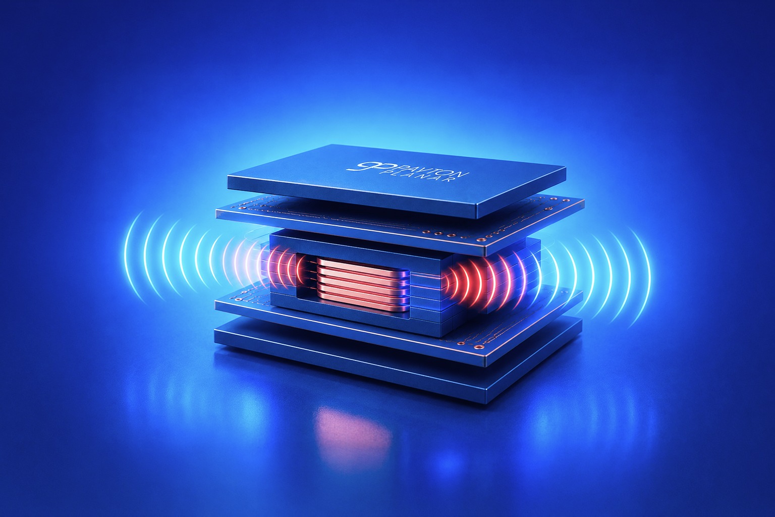 You've finalized the schematic, hit the efficiency target, and the prototype is running. Then the pre-compliance test reveals a conducted emissions spike at 500 kHz that pushes you over the CISPR 32 Class B limit by 12 dB. The next three weeks are spent adding CM chokes, Y-capacitors, and shield cans - none of which were in the original bill of materials.
In a significant proportion of these cases, the root cause is not poor filter design, it's a transformer that injects noise faster than the filter can suppress it. The geometry of the magnetic component determines how much common-mode current crosses the isolation barrier, how much flux leaks into adjacent circuits, and how much differential-mode noise appears on the power rails.
How Magnetics Generate Electromagnetic Interference
There are four primary EMI generation mechanisms in transformer-based converters:
- Common-Mode (CM) Noise: High dV/dt switching events on the primary couple capacitively through the inter-winding capacitance into the secondary. This displacement current flows through Y-capacitors to ground, appearing as CM conducted emissions on the mains. In a 400V bus converter at 400 kHz with 100 pF inter-winding capacitance, the injected CM current at the fundamental can exceed 100 mA, well above CISPR 32 and IEC 61000-3-2 limits.
- Differential-Mode (DM) Noise: Switching current ripple and its interaction with the converter source impedance generates voltage harmonics on the power rails. Transformer leakage inductance participates by creating voltage spikes during switch transitions.
- Radiated EMI from Flux Leakage: Magnetic flux escaping the core couples inductively into nearby PCB traces, cables, and structures. In open-wound transformers, near-field H-field emissions can violate radiated limits without any conducted path at all.
- Conducted Noise from Winding Resonances: Parasitic capacitance within and between windings resonates with inductance at frequencies within the regulatory band (150 kHz - 30 MHz for CISPR 32), creating high-Q noise peaks that are difficult to filter.
Wire-Wound vs. Planar: Structural EMI Comparison
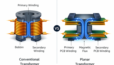
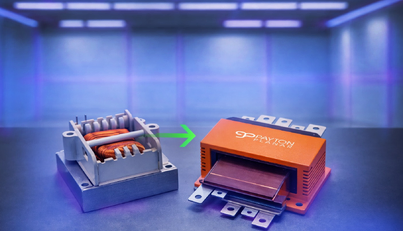
Wire-wound transformers have a fundamental EMI disadvantage: their parasitic values vary 30-50% across a production lot because the winding geometry depends on manual processes. Planar magnetics, defined by PCB Gerber files, deliver parasitic values repeatable to ±10% - the foundation of a reliable EMI design process.
| EMI Characteristic | Wire-Wound | Planar (PCB-Based) | Planar Advantage |
|---|---|---|---|
| Inter-winding capacitance | Variable (±30-50%) | Repeatable (±10%) | Predictable CM noise |
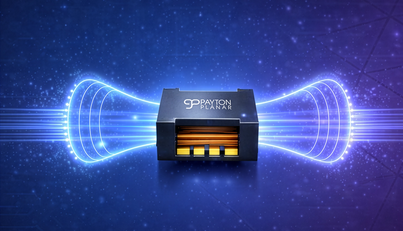
| Flux containment | Open core - leakage escapes | Closed core - flux contained | Lower radiated H-field |
| Winding loop area | Large - coiled wire | Small - PCB traces | Lower radiated emissions |
| Faraday shielding | Difficult to implement | PCB layer - easy to add | 20–30 dB CM reduction |
| Leakage inductance | Variable, uncontrolled | Defined by geometry | Repeatable DM filtering |
| Production consistency | Low - manual winding | High - automated PCB | Reliable EMC compliance |
Faraday Shielding: The Most Effective CM Noise Mitigation
The Faraday shield is the single most impactful technique for reducing common-mode noise in isolated planar converters: a grounded copper layer inserted between primary and secondary that intercepts displacement current before it crosses the isolation barrier. Typical result: 20-30 dB reduction in conducted CM emissions, often eliminating the need for external CM chokes.
Correct Faraday shield design requires:
- Single, unbroken copper layer: The shield must have no complete electrical loop, a circumferential gap prevents circulating currents that would make it act as a shorted turn, introducing losses.
- Full-width coverage: The shield layer must be as wide as possible to intercept the complete electric field between primary and secondary.
- Low-impedance ground connection: The shield connection to safety/chassis ground must be short and direct, not a trace routed across the board.
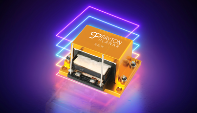
- Correct placement in the PCB stackup: The shield layer is placed directly between the primary and secondary winding layers. Adding it typically requires one additional PCB layer.
Flux Leakage and Radiated Emissions
Not all core geometries offer equal flux containment. Core selection directly impacts near-field H-field radiation:
- EE core: Most common; moderate flux containment. Adequate for most applications with proper winding balance.
- ER / EQ core: Better enclosure of the winding - less exposed conductor area, lower near-field H-field emissions.
- Pot core: Highest flux containment - winding entirely enclosed. Maximum EMI suppression; reduced thermal access to winding.
- Distributed air gaps: Spreading the core gap across multiple smaller gaps reduces fringing flux intensity at any single point, lowering localized eddy current coupling into nearby conductors.
A solid ground plane beneath the transformer footprint provides a controlled return path for any flux-induced currents in the PCB, significantly reducing effective loop area for radiated emissions. Via fencing around the transformer footprint adds shielding above a few hundred megahertz.
Differential-Mode Noise: Leakage Inductance as a Filter Element
Leakage inductance in a planar transformer provides first-order differential-mode filtering of switching ripple. Because it is determined by PCB geometry, it is highly repeatable across production. A known, stable leakage inductance can be incorporated into the DM filter design as a passive element, reducing the size or count of external filter components.
System-Level EMC Design Practices
- Ground plane strategy: Maintain solid, unbroken ground planes beneath the transformer footprint and adjacent converter circuitry. Avoid routing non-ground signals under the transformer.
- Minimize high dI/dt loop area: Keep the switching current loop as small as possible. Planar magnetics compact geometry makes this naturally easier than with wire-wound components.
- Faraday shield as standard practice: For isolated converters with CM noise requirements, include the Faraday shield layer in the initial stackup rather than adding it as a fix during compliance testing.
- Spread-spectrum switching: Reduces peak spectral density of conducted emissions by modulating switching frequency over a narrow range. Complements structural EMI reduction.
- Pre-compliance near-field probing: Use an H-field probe to localize noise sources before the formal compliance test. Identifies whether the transformer, switching loop, or output filter is the dominant emitter, enabling targeted fixes rather than blanket overdesign.
EMC Is a Magnetics Design Problem
The EMI filter at the input of your converter is not the primary line of defense against conducted and radiated emissions. The transformer is. Its geometry determines the CM noise source impedance, DM noise spectral content, and near-field H-field environment for everything around it.
Planar magnetics offer a structural starting point fundamentally superior to wire-wound for EMC: contained flux, reproducible parasitics, and a PCB platform that enables intentional Faraday shielding. Reach out to Payton Planar to discuss EMC-aware magnetics design for your application.